Apple Pies and Power Converter Efficiency
October 7, 2021
This blog post was first published by United Silicon Carbide (UnitedSiC) who joined the Qorvo family in October 2021. UnitedSiC is a leading manufacturer of silicon carbide (SiC) power semiconductors and expands Qorvo’s reach into the fast-growing markets for electric vehicles (EVs), industrial power, circuit protection, renewables and data center power.
It’s always tempting to start blogs with ‘motherhood and apple pie’ statements, like the list of benefits of better power conversion efficiency. Higher is obviously an advantage, but sometimes the net gains are mis-stated – a little heat from household electronics makes your central heating work less hard in a cold climate, perhaps with an overall benefit in energy use and cost, with a relatively inefficient boiler. The same can be said of incandescent lights – they are very efficient heaters when you need warmth anyway.

Other users do see a major benefit though – in warm locations, heat generated makes air conditioning work harder, multiplying up costs and in industry, server farms for example now exceed 1% of global energy demand and every fraction of a percentage point of efficiency improvement represents major cost savings and reduced environmental impact. Sometimes efficiency gains reach a ‘tipping point’ where benefits start to multiply, as with EVs, where improvements mean smaller and lighter power converters resulting in less energy demand and longer range.
So, engineers relentlessly pursue decimal points of efficiency increase, often judging whether the risk of designing with a new unfamiliar topology with a promised fractional improvement will yield a total cost of ownership that is lower over some arbitrary timescale. Convincing yourself that there is even an improvement gets harder as you improve efficiency, a creditable ±0.1% error in measurement of power in and out can mean calculated losses could be 40% more or less than the real values, when efficiency is already at around 99.5%. When power in is AC with distortion and a less than perfect power factor and DC power out has a residual noise component to confuse DVMs, it gets worse still. It’s now common to resort to calorimetric methods to actually measure heat output rather than extrapolate from electrical measurements.
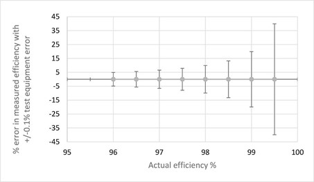
Figure 1. Even ±0.1% test equipment accuracy gives wide variation in efficiency measurement accuracy at high efficiency levels
One relatively low-risk option to increase efficiency of a power converter is to just improve on the semiconductors already designed-in. MOSFET-based converters can be upgraded to use newer devices with lower on-resistance and perhaps lower switching energy requirements, with due consideration to changed EMI emissions. However, to get leverage off the latest wide band-gap devices such as SiC MOSFETs or GaN HEMT cells, wider changes to a circuit are necessary, particularly to the gate drive. If the existing circuit is IGBT-based, you are looking at a ground-up re-design to use wide band-gap devices.
The gate drive issue has to do with voltage levels – for full enhancement, SiC MOSFETs need an on-state drive which is significantly higher than Si-MOSFETs and is perilously close to the absolute maximum rating of the device and must be carefully limited. The high swing in voltage between on- and off-states also demands some drive power as the gate capacitance is charged and discharged each cycle. Also, the threshold voltage is variable and has hysteresis, making an optimum drive difficult. GaN HEMT cells in a way are the opposite, the gate threshold voltage and absolute maximum is very low and again the drive circuit must be carefully controlled to avoid overstress and failure.
If the power converter circuit requires reverse or third quadrant conduction, the characteristics of the body diode in a SiC MOSFET are important and can lead to excessive losses due to its significant recovery energy and forward voltage drop. GaN devices have no body diode and conduct in reverse through the channel but with a high voltage drop in the dead-time before the channel is actively enhanced through the gate drive. If the gate is driven negative for the off-state, the drop during ‘commutation’ is even higher.
A way to get the best of all worlds is to consider SiC FETS, the cascode combination of a Si-MOSFET and a SiC JFET. The devices have the easy, non-critical gate drive of a Si-MOSFET but better performance figures of merit RDS(on) x Aand RDS(on) x EOSS than SiC MOSFETs and GaN HEMT cells. There is a robust inherent avalanche capability and self-limiting short-circuit current, and the body diode effect is similar to a low voltage Si-MOSFET with low forward drop and fast recovery. This all means that a SiC FET can often be simply dropped-in to a Si-MOSFET or even an IGBT slot for an instant boost in efficiency. The speed of SiC FETs can’t be controlled to limit EMI and stress simply by adjusting gate drive resistance as with other technologies but with these ultra-fast devices, overshoots and ringing are effectively limited by small RC snubbers which also simplify parallel operation of devices. When replacing IGBTs, switching frequency can be increased without undue dynamic losses, to get the advantage of smaller, lighter, and lower cost magnetics.
SiC FETs are a secure way to get better efficiency out of all common conversion topologies with all the consequent benefits. They say that if you can’t stand the heat then, well, stop baking apple pies (not an option), but you could switch to SiC FETs in your converter designs.
Have another topic that you would like Qorvo experts to cover? Email your suggestions to the Qorvo Blog team and it could be featured in an upcoming post. Please include your contact information in the body of the email.