Distributed Amplifiers Are a Unique Circuit in High Frequency Microwave Engineering
October 22, 2019
This blog post was first published by Custom MMIC who joined the Qorvo family in February 2020. Custom MMIC is known for its best-in-class die and packaged components, which augment our power amplifiers to enable multi-chip modules for a broad range of defense, aerospace and commercial applications.
 The distributed, or wideband, amplifier is a unique circuit in the field of high frequency microwave engineering. Its architecture can often be misunderstood, however, and this confusion can sometimes result in a non-optimal use of the amplifier. In this note, we will explain the inner workings of a distributed field effect transistor (FET) amplifier and how best to use this circuit in a microwave system.
In a traditional FET amplifier design, the active devices are individually tuned and matched with lumped or distributed networks to obtain a specific frequency response. Designers of such amplifiers must make tradeoffs relative to bandwidth, efficiency, gain and flatness such that a maximum achievable bandwidth is typically no more than one to two octaves.
When a larger bandwidth is needed, designers turn to distributed amplifiers. The concept of a distributed amplifier was first conceived by William S. Percival in 1936[1] and popularized in 1948 by Ginzton, Hewlett, Jasberg and Noe[2]. The distributed amplifier functions by creating a pair of transmission lines. One transmission line connects the inputs, or gates, of the devices in a FET based amplifier, and is then terminated with a resistor. The other transmission line connects the outputs, or the drains, in a FET based amplifier, and provides the output of the amplifier. A distributed amplifier designer must take care to match the delay on the input and output lines in order to ensure the output of each transistor sums in phase with the other devices in the chain. The actual impedances seen by each individual FET vary, however the input and output are both matched over a wide bandwidth to some characteristic impedance Z0, which is typically 50 ohms in microwave applications. This approach makes it possible to achieve performance over an extremely wide bandwidth that is limited primarily by the cut-off frequency (fT) of the technology used to develop the amplifier, rather than the one to two octave practical limitations of an amplifier utilizing a lumped element matching network.
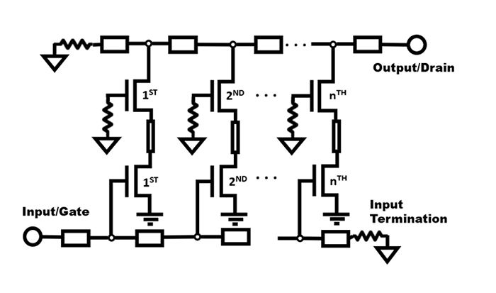 Figure 1: Conceptual n-stage distributed amplifier with a cascode configuration
In addition to this distributed approach, many MMIC-based distributed amplifiers use a cascode configuration which consists of a common source FET as the input to the amplifier and a common gate FET driven by that input stage as the output. This architecture offers several advantages, including higher input and output impedances, higher gain and broader bandwidth. A conceptual n-stage distributed amplifier with a cascode configuration is shown in Figure 1.
Understanding this architecture is critical in understanding its advantages and disadvantages. As with any amplifier, performance characteristics like gain, return loss, noise figure, power, linearity and efficiency are all very important, but when selecting a distributed amplifier for your application there are several other factors to consider.
First, transmission lines generally have more loss at higher frequencies than at lower frequencies, mainly due to the skin depth of the metal. Such a phenomenon occurs in distributed amplifiers as well, which can result in a gain that slopes down as the frequency increases. Since most wideband systems require the gain to be flat across a wide frequency range, the selection of a distributed amplifier with negative gain slope will require additional components to equalize the gain, and this solution is not always welcome. However, it is possible to create a flat, or even positive gain slope with respect to frequency. For example, as shown in Figure 2, the CMD192C5 distributed amplifier has a positive gain slope with respect to frequency from DC-20 GHz. Such performance offers considerable advantages to a wideband system designer by eliminating some of these equalization stages and reducing the size, power and complexity of the design implementation. In the case of even wider band systems where positive gain slope may not be achievable, a flat response with respect to frequency offers similar advantages. The CMD304, for example, is a DC-67 GHz distributed amplifier with a flat gain response with respect to frequency, as shown in Figure 3.
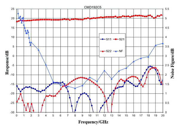 Figure 2: S-parameters and noise figure versus frequency for the CMD192C5 distributed amplifier
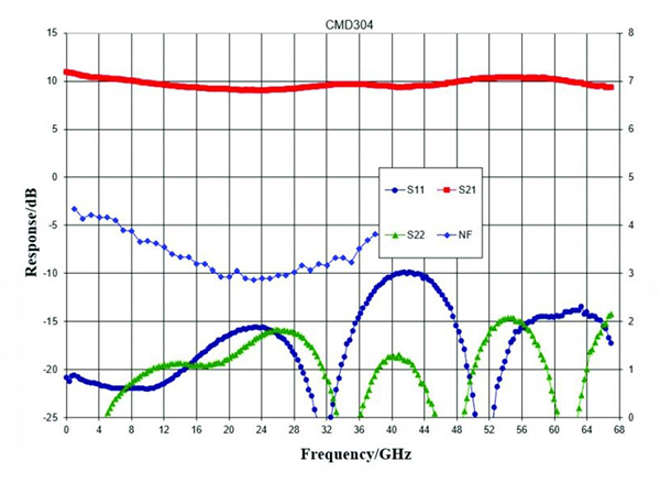 Figure 3: S-parameters and noise figure versus frequency for the CMD304 distributed amplifier
Second, another amplifier characteristic of importance as shown in Figures 2 and 3 is the low frequency noise figure. In a distributed amplifier, the noise figure is not only impacted by the channel and gate noise as it is in other amplifier topologies, but it is also impacted by the thermal noise of the input termination. The noise from this termination is filtered before it reaches the output such that it only has a significant impact below B/n where n is the number of amplifier stages and B is the bandwidth of the device[3]. Returning to Figure 2, it is apparent that the noise figure of the CMD192C5 below 4 GHz is increasing due to noise from the input termination. In Figure 3, however, the low frequency noise figure of the CMD304 is much flatter than the CMD192C5 even at 1 GHz, the lowest measured frequency point for the CMD304. The reason: the CMD304 has many more FET stages than the CMD192C5. Therefore, if low frequency noise figure is an important system consideration, choosing a distributed amplifier with more stages is a preferred solution. Additional techniques can be employed to further reduce the effect of this termination on the low-frequency noise figure and future products featuring these techniques will provide good noise performance well below the B/n limit.
Next, some wideband applications also require the amplifiers to have low additive phase noise. Such amplifiers are critical for many applications where received power levels can be very low, such as high-end direct conversion receivers or radar systems. In these wideband systems, designers must use an amplifier which does not contribute to the system phase noise, as the additive noise could potentially obscure the desired signal after mixing with the LO. However, it is well known that the additive phase noise of FET-based amplifiers can be quite high. Therefore, to achieve low-phase-noise distributed amplifiers, circuit designers turn to hetero-junction bipolar transistor (HBT) processes. HBTs are known to have very low 1/f noise, which gives amplifiers of this type extremely low additive phase noise. The CMD275P4 is an example of an extremely broadband low-phase-noise amplifier. When compared to a similar broadband part designed on a pHEMT process, this component which was developed on an HBT process shows about a 20 dBc/Hz improvement in phase noise at a 10 kHz offset.
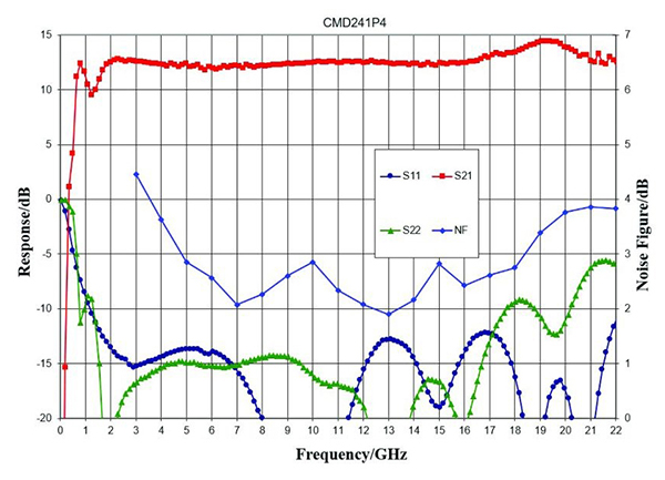 Figure 4: S-parameters and noise figure versus frequency for the CMD241P4 distributed amplifier
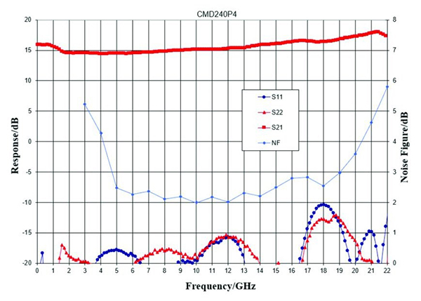 Figure 5: S-parameters and noise figure versus frequency for the CMD240P4 distributed amplifier
In addition to the RF characteristics of the device, it is important to consider how the DC power will be supplied to a distributed amplifier and how the bias circuit could affect performance. In applications where size of implementation is critical and performance to very low frequencies is not necessary, most designers will select a MMIC such as the CMD241P4 with an on-chip bias choke and DC blocking capacitors on the RF input and output. While reducing the total footprint required by the amplifier, these on-chip components limit performance, not only because the DC blocking capacitors will limit the low end, but also because the higher resistance of the on-chip bias choke - when compared to a high-quality conical inductor - affects the high frequency performance as well. In order to understand the limitations, Figures 4 and 5 show the performance of CMD241P4 with on-chip bias structures (Figure 4) along with the CMD240P4, which features the same amplifier design with off-chip biasing (Figure 5).
While small size and ease of implementation are goals of almost any system, in some designs it is critical to get as close to actual DC performance as possible without limiting the high-frequency performance, even at the expense of board space. There are many distributed amplifiers designed for these applications which require an off-chip bias choke and DC blocking capacitors on the RF lines. This architecture allows the system designer to obtain the performance needed by selecting components which will provide the broadest possible performance. Selecting the right external components must be done very carefully to ensure proper performance of the distributed amplifier. First, the designer must select a broadband inductor that can handle the bias current required for the device with sufficient margin and one which does not have any in-band resonances that will affect performance. The DC blocking capacitors also need to be selected without any in-band resonances while being able to pass the lowest frequency required by the application.
With many different factors to consider in addition to the typical amplifier parameters, it is critical that a wide variety of distributed amplifier options be available to wideband systems designers. Custom MMIC’s growing distributed amplifier portfolio includes high power, low noise, extremely wide bandwidth and low phase noise options. Most of these amplifiers exhibit flat or positive gain slope with respect to frequency and there are options for both on-chip and external biasing. This breadth of offerings ensures that wideband systems designers always have an option to meet the ever-increasing demands of high performance across extremely wide bandwidths.
References
- W.S. Percival, “Thermionic Valve Circuits,” British Patent Specification no. 460,562, filed 24 July 1936, granted January 1937. 2.E.L. Ginzton, W.R. Hewlett, J.H. Jasberg, J.D. Noe, “Distributed Amplification,” Proceedings of the IRE, vol. 36, no. 8, August 1948.
- A. Kopa, A.B. Apsel, “Distributed Amplifier with Blue Noise Active Termination,” IEEE Microwave and Wireless Components Letters, vol. 18, no. 3, March 2008, 203.
Have another topic that you would like Qorvo experts to cover? Email your suggestions to the Qorvo Blog team and it could be featured in an upcoming post. Please include your contact information in the body of the email.