ESD Design Strategy for Mobile Devices: Your Tools for SEED (Part 2 of 3)
August 2, 2018
This is the second blog in a three-part series explaining various aspects of electrostatic discharge (ESD) and system-level ESD design for mobile devices.
In Part 1, we introduced the basic concepts
of ESD and system-efficient ESD design (SEED). This blog gives you all
the necessary pieces you should have in your toolkit for SEED. Part 3 will
cover how to use SEED methodology along with modeling and simulation to
optimize your system-level handset designs.
To refresh, SEED is…
…a co-design methodology that comprehends both on-board and on-chip ESD protection to analyze and achieve system-level ESD robustness. This approach requires a thorough understanding of the interactions between external ESD pulses, full system-level board design, and device pin characteristics during an ESD stress event.
On-board ESD protection devices
As a general strategy, you can use a number of protection components on the PC board to protect the end-product from an ESD event. These protection components can include the following:
Passive and active components, like:
- Series resistors
- Decoupling capacitors
- Ferrite beads
- Suppression devices like electromagnetic interference (EMI) / ESD filters
- Transient voltage suppressors (TVSs)
TVS components:
- Polymer varistors
- Ceramic varistors
- Spark gaps
- Silicon diodes
However, there are several things to keep in mind when using these components:
- Resistors, capacitors, inductor-capacitor (LC) filters and ferrite beads work well in attenuating indirect or secondary ESD stress in a system. To be effective, these components need to be placed as close as possible to the ESD stress victim (module pins).
- You can use series resistors with decoupling capacitors (resistor-capacitor [RC] filters) or with voltage clamps.
- Capacitors provide decoupling. It’s best to choose capacitors with high voltage ratings, high resonant frequency, low resistance and low inductance. Make certain to minimize trace lengths when connecting capacitors.
- LC filters block transients and EMI.
- Series ferrite beads attenuate EMI and ESD on power supply lines.
- Varistors change from high standby values to a very low conducting value, thus absorbing the ESD energy and limiting the ESD-induced voltages. They typically have high trigger voltages (hundreds of volts) and clamping voltages that can reach 100 V. They have very low capacitance but can display significant leakage currents after prolonged ESD stress.
- Depending on the type of interface to be protected, silicon-based TVS diodes can also have low capacitance and much lower dynamic resistance values compared to other TVS components. They have high ESD absorption capabilities (i.e., once the ESD strike is absorbed, the protection device returns to its high impedance state very quickly). TVS diodes for high-speed/RF applications can offer very low trigger voltages (less than 100 V) and clamping voltages (less than 20 V), with excellent response time.
But beware: Capacitance of the off-chip protection device will cause
mismatches in the RF pathway. To compensate for these mismatches, designers
need to adjust their matching networks in the RF and antenna paths.
Glossary of Terms
- C: capacitor
- CS: shunt capacitor
- EMI: electromagnetic interference
- ESD: electrostatic discharge
- FCC: Federal Communications Commission
- GND: ground
- HPF: high pass filter
- IC: integrated circuit
- IEC: International Electrotechnical Commission
- L: inductor
- LC: inductor-capacitor
- LS: shunt inductor
- PC: printed circuit
- PCB: printed circuit board
- RC: resistor-capacitor
- RF: radio frequency
- RFFE: RF front end
- Rx: receive
- SEED: system-efficient ESD design
- TVS: transient voltage suppressor
- Tx: transmit
- VL: inductor voltage
A little more about transient voltage suppressors (TVSs)
TVS diodes are one of the go-to components for ESD protection. They operate by shunting excess current when the induced voltage exceeds the avalanche breakdown voltage. They are a clamping device, suppressing all overvoltages above the breakdown voltage. They automatically reset to the off state when the overvoltage goes away but absorb much more of the transient energy internally.
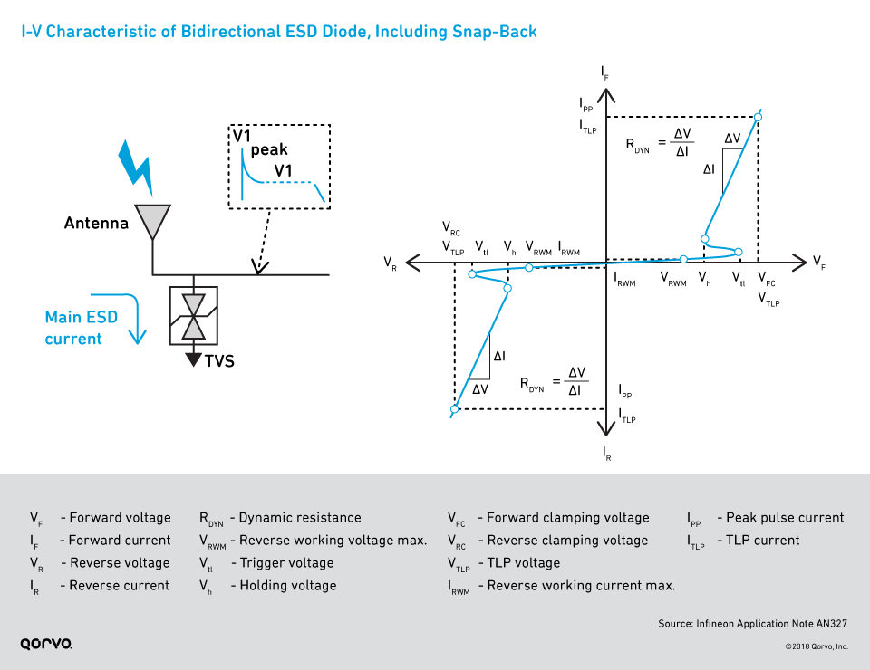
A TVS diode may be either unidirectional or bidirectional. A bidirectional diode can be represented by two mutually opposing avalanche diodes in series with one another, as shown below, and connected in shunt configuration relative to the pin to be protected. These devices are manufactured as a single packaged component.
For ESD protection in RF applications, it’s mandatory to keep the TVS diode capacitance as small as possible. This avoids a detuning of the input matching, and as a result, the protection device will create less harmonic distortion.
The following figure shows the current-voltage (I-V) curve of a bidirectional TVS diode. As you can see, the TVS is symmetrical with respect to the origin, and its ESD protection capability is provided for a positive and negative ESD strike.
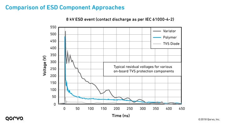
The following graph compares the residual voltages of a varistor, polymer and TVS diode in response to an ESD strike. As you can see, today’s silicon-based TVS diodes are the most effective approach to ESD strikes.
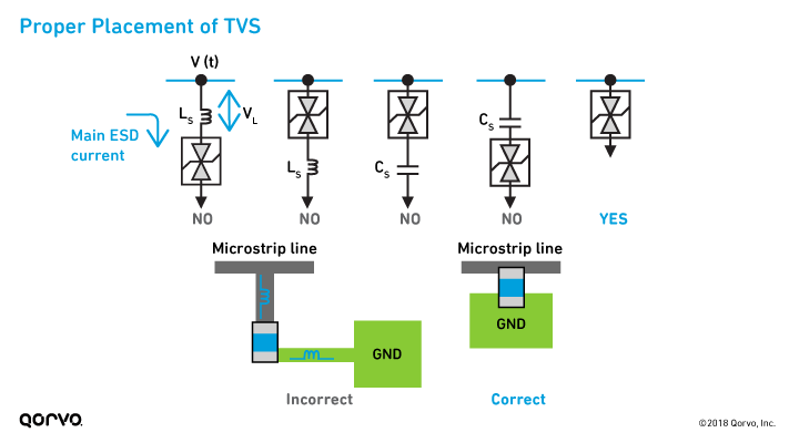
The importance of on-board TVS diode placement
However, where you place the TVS makes a big difference. ESD protection won’t be as effective if you don’t design the circuit properly. Keep in mind these general guidelines:
- Take care when developing the PC board so traces are not lengthy, as this provides unwanted inductance.
- Remember: Capacitors in series with the TVS device break down the primary ESD current path, while any RF inductance added to the primary ESD current path increases the total impedance in the residual path.
- If you place a TVS properly, you don’t need all the other ESD
components.
So what is the proper placement? As shown in the following image, you should:
- Use only the TVS.
- Don’t place the TVS before or after a capacitor or inductor.
- Make sure there’s no trace. When you place the TVS, it should be right between the RF path and ground.
Getting grounded: The mechanical factor
To mitigate ESD events, it’s essential to properly ground every aspect of the finished end-product — the PC board, all IC chips and components, the housing, cover, etc. Make sure you consider all the following aspects in your end-product’s grounding:
- All metal pieces must connect to the system ground via a low-impedance path.
- Floating metal parts are ESD hazards.
- All metal items must be grounded or changed to plastic, where applicable.
- Multiple interconnected PC board designs can result in highly resistive, inductive system grounds. You should pay special attention to the antenna protection when the primary TVS and the RF module are placed on different PC boards.
Primary and secondary ESD protection
Understanding primary and secondary ESD protection is a fundamental part of SEED methodology. Typically:
- Primary protection is done on the board and is called the primary clamp.
- Secondary protection is done on the chip and is called the secondary clamp.
Co-design of the primary and secondary ESD protection stages is the fundamental concept of SEED methodology.
The following figure shows a high-level, basic view of the primary and secondary clamp for ESD protection in an RF front end (RFFE).
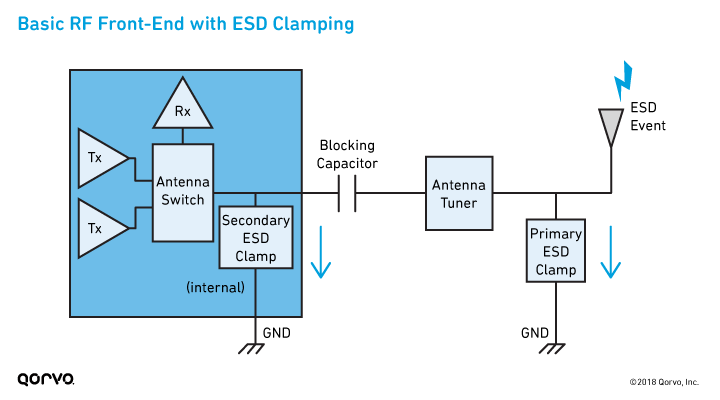
Note: Some system designs require an additional on-board secondary clamp located before the IC to mitigate any residual ESD charge a component pin might see.
Let’s look a bit closer at primary and secondary protection:
- Primary protection (on-board): This protection may include clamping components like shunt inductors or TVS components (diodes, varistors and spark gaps). These primary clamps shunt large ESD currents. Primary clamps should focus on external connections and other interfaces exposed to direct ESD energy ingress. They also play an important role in reducing the residual ESD stress that appears at the IC component pins.
- Secondary protection (on-chip): This protection is used to clamp any residual ESD stress that builds up at the device pins. The shape of the ESD transient is largely dependent on the on-board primary clamp characteristics and PC board design.
Co-design of the primary and secondary ESD protection stages — that is, of the on-board and on-chip protection — is the fundamental concept of SEED methodology. These two stages provide the necessary protection where the current-carrying capabilities on both branches are balanced by a serial impedance.
Simulating and analyzing the two protection stages helps board designers select the proper on-board protection clamping levels, to ensure peak residual pulses reaching the ICs are effectively handled. SEED protection design using simulation requires putting together International Electrotechnical Commission (IEC) stress models, TVS and IC interface pin models based on SEED parameters, and an isolation impedance circuitry (i.e., on the PC board). We'll go into the details of how to simulate and analyze your design for SEED in Part 3.
Protection strategies for the RF front end (RFFE)
Different applications will have different demands for ESD protection. One approach might be good enough for your application, but it may not work for others. Ultimately, the design you use has to pass FCC and IEC testing, so that your product can be certified and sold.
Let’s look at several strategies you could employ for ESD protection in the RFFE.
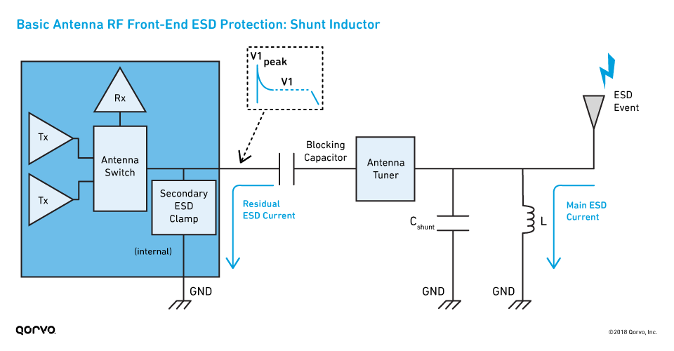
Strategy #1: Basic protection – Shunt inductor
The most basic approach uses a shunt inductor. As shown in the following figure, the inductor (L) is the main shunt element for the ESD current pulse. This inductor should be in the low nano-Henry range (<20 nH) to be an effective ESD protective solution. However, it does add insertion loss, which creates some RF performance challenges. A shunt capacitor is typically introduced for RF matching purposes, not ESD protection.
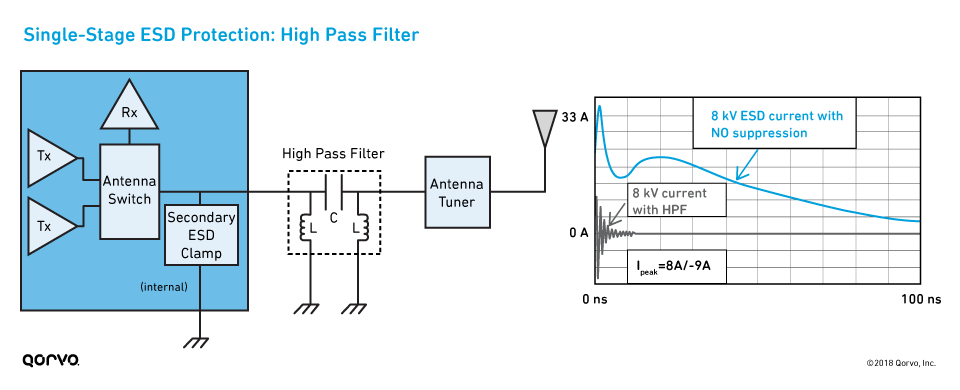
Strategy #2: Single-stage high pass filter
A second approach uses a single-stage high pass filter (HPF), as shown in the figure below. However, this may not be the most effective approach.
Pros:
- Provides good full-bandwidth ESD coverage.
- Can reasonably reduce the ESD pulse amplitude while allowing the cellular range to pass through.
Cons:
- Can produce high residual voltages (Vpeak >100 V).
- Low inductance is required to ensure optimal performance results (which means RF versus ESD performance trade-offs).
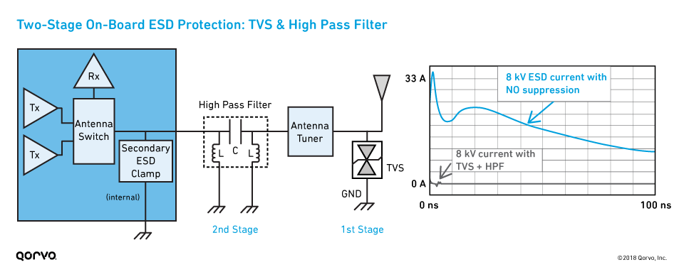
Strategy #3: Two-stage ESD protection
A third approach uses two stages of ESD protection, as shown in the next figure. This approach uses a TVS as primary protection and an HPF for secondary ESD protection to capture the residual stress.
As you can see from the image below:
- The first stage (TVS) clamps the voltage <20 V, which reduces the peak voltages to <50 V.
- The HPF in the second stage further reduces residual voltage pulses, clamping at <10 V. This reduces the peak voltages <20 V.

The best approach for ESD protection
Ultimately, you’re trying to reduce the voltage that the IC would see in an ESD strike; the goal is to reduce all the peak voltages before they hit the IC. We believe an ideal ESD strategy is the two-stage approach, with the first stage using a TVS element (TVS diodes) and the second stage using an HPF network.
Benefits:
- It improves your board-level ESD protection and gives you the best opportunity to pass IEC testing.
- It further reduces ESD pulse amplitude and residual voltages along the RF path.
- Bidirectional TVS diodes help protect against both positive and negative pulses.
- Any residual voltage pulses are clamped by the high pass filter.
- Therefore, it provides optimum protection to the component pins.
Next up: Implementing SEED in your system design
It isn't uncommon to have ESD problems late in the design cycle when the mobile device doesn’t pass certification tests. We’ve learned that the best approach is to plan for ESD protection and the RF design from the outset — before designing the full board — because it reduces churn, design spins and certification headaches.
Now that you have the background and the tools to address ESD, our last blog in this series will talk about SEED methodology in detail and how you can incorporate it
into your system-level designs.
Read all the blogs in our series about overcoming ESD challenges in mobile devices:
- Part 1: Get Grounded: What You Need to Know About ESD and RF Devices
- Part 2: ESD Design Strategy for Mobile Devices: Your Tools for SEED (this post)
- Part 3: SEED Methodology for Optimizing an ESD RF Front-End Design
Have another topic that you would like Qorvo experts to cover? Email your suggestions to the Qorvo Blog team and it could be featured in an upcoming post. Please include your contact information in the body of the email.