Model-Based GaN PA Design Basics: GaN Transistor S-Parameters, Linear Stability Analysis and Resistive Stabilization
August 28, 2019
This is the fourth blog in an ongoing series looking at the importance of GaN HEMT nonlinear models for rapid power amplifier (PA) design success.
Introduction
S-parameter matching is used to maximize gain and gain flatness in simple linear RF/microwave amplifier designs. This same S-parameter data is used to develop matching and biasing networks that address amplifier stability. This blog discusses the importance of using modeling for basic S-parameter and stability analyses in the gallium nitride (GaN) power amplifier (PA) design process. It introduces the use of models and resistive stabilization techniques to help avoid device instabilities that can affect nonlinear and linear simulations.
In this blog, we limit our attention to a simple two-port stability analysis derived from linear S-parameter calculations. We will use a nonlinear Qorvo GaN power transistor model from the Modelithics Qorvo GaN Library, in combination with simulation templates and Keysight Advanced Design System (ADS) software.
Model-Based GaN PA Design Basics
Qorvo and Modelithics have teamed up to explain how nonlinear models and the Modelithics Qorvo GaN Library can improve your PA designs.
Catch up on the first blogs here:
- Part 1: GaN HEMT Models 101
- Part 2: What's in an I-V Curve?
- Part 3: The What and Why of Intrinsic I-V Waveforms
Stability Explained
Stability refers to a PA’s immunity from possible spurious oscillations. Oscillations can be full power, large-signal problems, or subtle spectral problems that might go un-noticed if not properly analyzed. Even unwanted signals outside your intended frequency range can cause system oscillations and gain performance degradation.
There are two types of stability and measures to analyze PA stability in your system.
- Conditional stability – a system design that is stable when the input and output see the intended characteristic impedance Z0 (50 Ohms or 75 Ohms) but may be subject to oscillations (exhibiting a negative resistance at the input or output port) for some other input or output impedance.
- Unconditional stability – a system that is stable in any possible positive real impedance inside of the Smith Chart. Note, that any system design can oscillate if it sees a real impedance that is negative (outside the Smith Chart). But generally speaking, if a system is defined as unconditionally stable, it is stable at all frequencies (where the device can have gain) and all positive real impedances.
Measures of stability
Let’s begin with the well-known “k-factor” and stability measure “b” to determine frequency ranges that cause instability at a given bias. These are given by the following equations1:
k = {1- |S11|2 - |S22|2 + |S11*S22 - S12*S21|2} / {2*|S12*S21|}
and
b = 1 + |S11|2 - |S22|2 - |S11*S22 - S12*S21|2
Unconditional stability is indicated by k > 1 and b > 0.
However, because this criterion requires two parameters to check for unconditional stability, a more compact formulation is given with the following “mu-prime” parameter2:
mu_prime = {1 - |S22|2} / {|S11 - conj(S22)*Delta| + |S21*S12|}
If mu_prime > 1, it indicates unconditional (linear) stability.
Matching and tuning to attain stability
As noted above, S-parameter data is used to develop matching networks to attain amplifier stability. Figure 1 shows a single-stage amplifier configuration and the key parameters that affect gain and stability. In the unconditional stability region maximum gain is achieved by setting Γs and ΓL to conditions attaining a simultaneous conjugate match at both ports.1
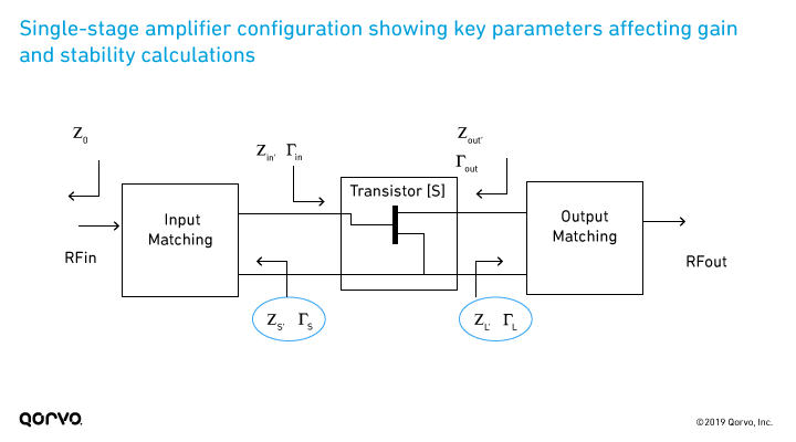 Figure 1.
Linear Stability Analysis
Stability Measurements of Untuned Transistor
Let’s consider an example. Figure 2 shows a simulation setup for linear S-parameter analysis of the nonlinear model for Qorvo’s T2G6003028-FS GaN HEMT device, included in the Modelithics Qorvo GaN Model Library.
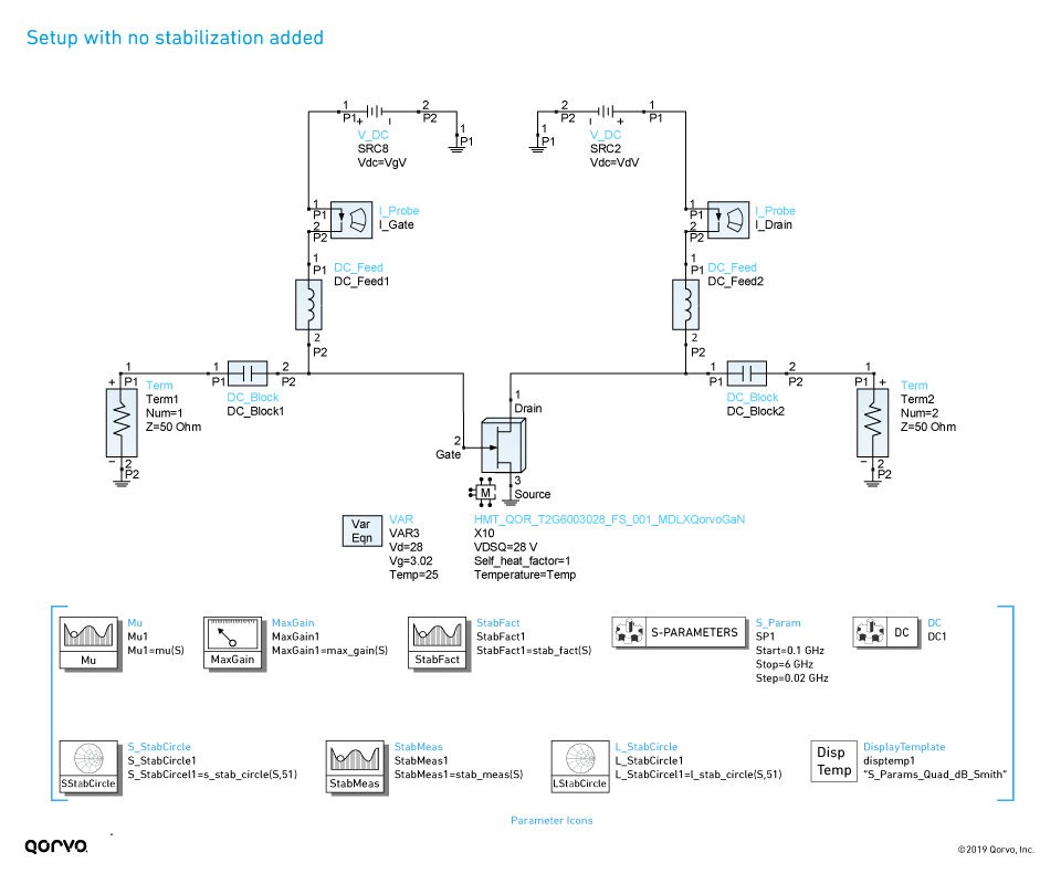 Figure 2.
Note: Bias condition for all simulations in this note is set to Vds = 28 V, Vgs = -3.02 V, which corresponds to a drain current of approximately 200 mA.
In the schematic above, icons represent parameters that can be calculated from device S-parameters, including stability k, b and mu_prime. The “MaxGain1” parameter is the maximum available gain. The “MaxGain1” parameter calculates the maximum available gain for frequency ranges where the device is unconditionally stable, and displays a value that is termed the maximum stable gain. This is calculated as simply |S21|/|S12| for regions of conditional stability.
Figure 3 shows the MaxGain1 parameter, the 50 ohm gain (S21 in dB) and stability factor k, measure b and mu_prime calculated from the schematic of Figure 2 (at m5). This plot shows that the stability measure b is > 0 and stability factor k > 1. The stability measurement parameters show a clear break point at about 1.85 GHz (m5). This is the transition frequency between conditional and unconditional stability regions. For 3.5 GHz the maximum gain indicated by this simulation parameter is approximately 18.4 dB (marker m3 in Figure 3). Note: The maximum available gain goes to 0 dB at about 10.4 GHz; this frequency is referred to as the maximum frequency or fmax. It is also a good practice to analyze stability from a very low frequency to at least fmax, which is why the frequency range for this example was set to sweep from 25 MHz through 12 GHz.
From this analysis, we can conclude the following:
- The device is unconditionally stable above 1.85 GHz.
- Frequencies below 1.85 GHz device are conditionally stable.
These S-parameters produced from the schematic simulation (Figure 2) are show in Figure 4. S11 and S22 are displayed on Smith charts, while polar charts are used for S21 and S12.
Notice the large difference between the gain for 50 ohm input and output (|S21| in dB) and the MaxGan1 value. This is due to the mismatch associated with S11 and S22 in a 50 ohm system.
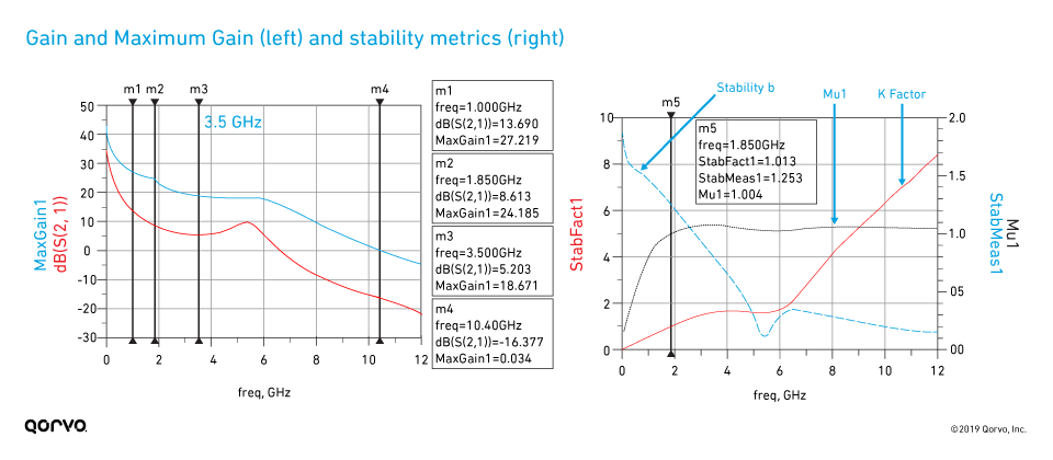 Figure 3.
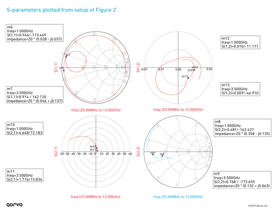 Figure 4.
Plotting the stability circles in the input and output planes provides additional insight. Also included in the schematic of Figure 2 are the icons for "S_StabCircle” and “L_StabCircle”, which correspond to calculations of stability circles in the input and output planes.
The meanings of these circles can be described as follows. In the case of the input stability circle at 100 MHz, indicated by marker 7 in Figure 5, each point along that circle represents a Γs value that will result in a Γout value equal to 1 according the following relation.
Γout = S22 + S12*S21*{Γs / (1-S11*Γs)}
Eq. 1
This circle sets a boundary between Γout < 1 and Γout > 1, the significance of which is that Γout > 1 corresponds to a negative resistance at the output port, which is a condition that can lead to an oscillation. The question then becomes whether the inside or outside of the circle is the unstable (Γout > 1) region. A quick check in the case of Γs = 0, which is the 50 ohm point. Note from Eq. 1, for this case Γout = S22, which is less than 1 at all frequencies being analyzed here. From this, we can conclude the outside of the circle is the stable region and the inside is the unstable region.
The explanation of the output stability circles is basically the same, except here we are plotting circles of points for ΓL for which Γin = 1, according to the Eq. 2. By a similar argument, we can conclude that it is the inside of the circles plotted on the right side of Figure 5 that correspond to the unstable regions. Note - the frequency plan of Figure 2 was reduced to show fewer circles in Figure 5 for clarity.
Γin = S11 + S12*S21*{ΓL / (1-S22*ΓL)}
Eq. 2
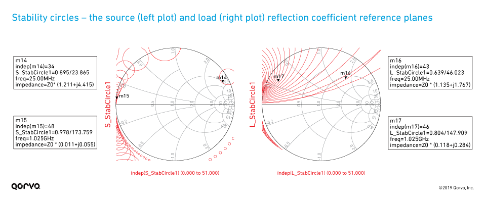 Figure 5.
Linear Stability Analysis
So, what if a device does not meet the requirements for unconditional stability, like in our example for frequencies below 1.85 GHz?
There are multiple matching methods to help stabilize your circuit. In this blog we describe two methods. One is resistive and the second is frequency-dependent stabilization.
- Resistive – uses matching resistors to provide stabilization
- Frequency-dependent – uses resistors, inductors and capacitors to provide stabilization
Resistive stability for microwave PA design
Matching resistors can be employed in our example to help stabilize high-gain, low-frequency transistors in most microwave applications. These resistors can be series or shunt at the input or the output, can be in the parallel feedback loop, or included in the bias networks. For PAs, we want to maximize output power, so it’s best to avoid resistors in the output network. Feedback amplifiers are outside the scope of this paper, so we will concentrate on the series and shunt resistors in the input network.
Figure 6 shows where both series and shunt resistors have been added in the input network. The values are tuned to achieve unconditional stability over the entire 0.025 to 12 GHz frequency range. The resulting stability measurements are plotted in Figure 7. These show the transistor has unconditional stability over the entire frequency range. Note, however, fmax dropped from 10.3 GHz to about 8.75 GHz. Comparing the maximum gain estimation in Figure 7 (design frequency of 3.5 GHz [12.3 dB]) with Figure 3 achieved without this stabilization (18.4 dB), we can see we have incurred a 6 dB degradation in maximum available gain. This is caused by adding a purely resistive input stabilization network. The S-parameters of the resistively stabilized device are displayed in Figure 8, with the overlaid S-parameters of the non-stabilized device. We can see that S11 and S12 have been affected over the entire frequency range, and S21 is also reduced with only minimal change in S22. It is gratifying to observe in Figure 9 that with the resistive stabilization network added, the stability circles are now all outside of the Smith Chart in both the source and load-planes.
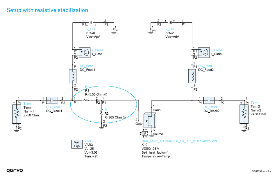 Figure 6. (Note: Analysis setup is the same as in Figure 2)
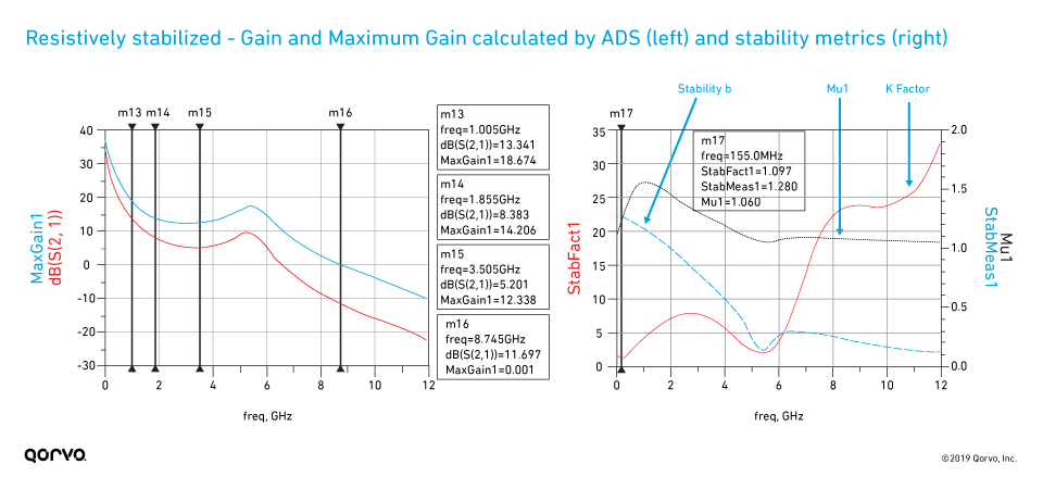 Figure 7.
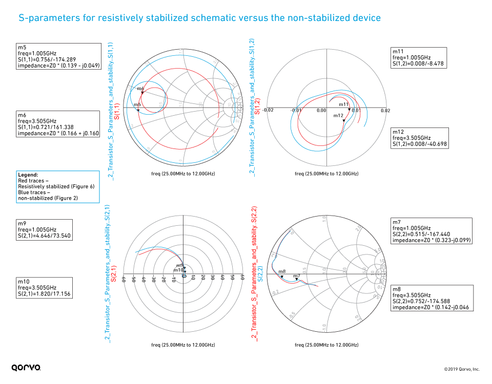 Figure 8.
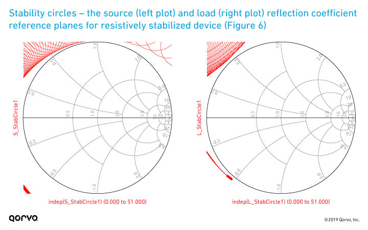 Figure 9.
Frequency-dependent resistive stability - Approach 1 (initial circuit)
If the design frequency is above 1.85 GHz (e.g., 3.5 GHz), we can implement a frequency-dependent resistive approach using the series-shunt stabilization network. Let’s see if we can mitigate the above gain penalty using this approach.
In Figure 10, a resistor (R1) has been incorporated into a modified gate bias network. Additionally, a capacitor (C3) has been placed across the series stabilization resistor (R1). The value of this capacitance can be tuned to adjust what frequency the series resistor (R1) is - effectively shorting it out (making it not “seen”). This can help increase the available gain.
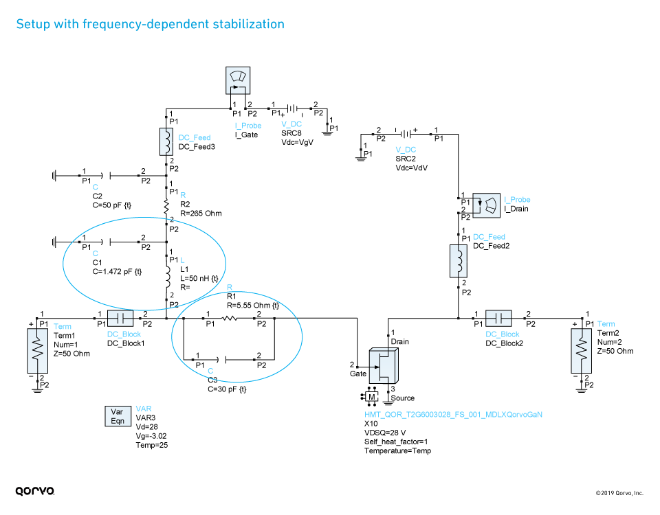 Figure 10.
The inductor (L1) and capacitor (C1) are used to create a low-pass filter. This prevents the resistor (R1) from being seen at higher RF frequencies, or lower frequencies for stabilization. The gain, stability and S-parameter analysis for this solution is shown in Figure 11, Figure 12 and Figure 13. As shown, the frequency-dependent stability network provides unconditional stability across the full frequency range, while reducing the impact on maximum available gain at 3.5 GHz. Note the gain at 3.5 GHz is now reduced by only about 1dB compared to the non-stabilized device, and also the fmax is about the same as the non-stabilized device (~10.4 GHz). In examining the S-parameter comparison to the non-stabilized device as shown in Figure 12, we see that, in contrast to the resistively stabilized device, the S-parameters are not altered over the entire frequency range, but rather only at lower frequencies, as desired. Figure 13 just confirms that none of the stability circles overlap with the Smith Chart in either the source or load planes as expected for an unconditionally stable circuit.
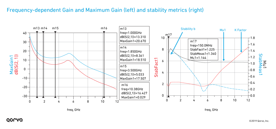 Figure 11.
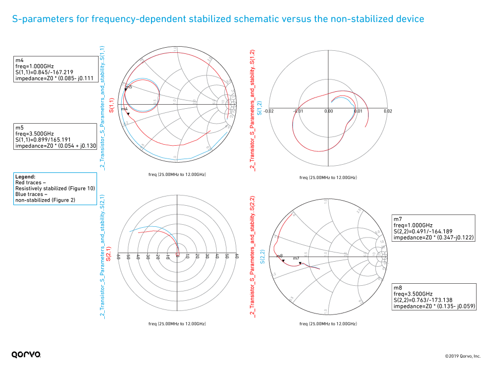 Figure 12.
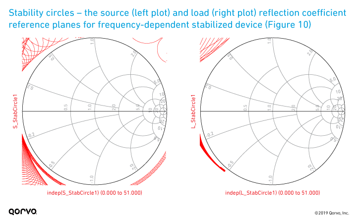 Figure 13.
Frequency-dependent stability – Approach 2 (preferred circuit)
While the above frequency-dependent stability solution seems to work well, it could have a problem in that the large 265-Ohm series resistor in the gate bias circuit could have too large of a voltage drop due to gate leakage current. Another circuit, that provides good stabilization and similar gain performance is shown below.
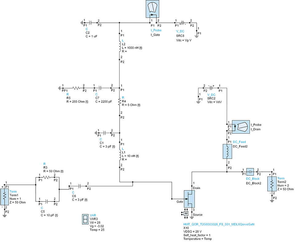 Figure 14.
As you can see from the below output measurements the above circuit offers good Gain as well as stability and, as an added bonus, will mitigate any potential leakage issues that may occur. Since there are many different GaN transistor design approaches the application note; GaN Bias Circuit Design Guidelines is another good resource that supports this approach.
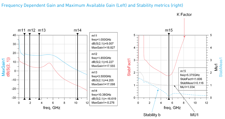 Figure 15.
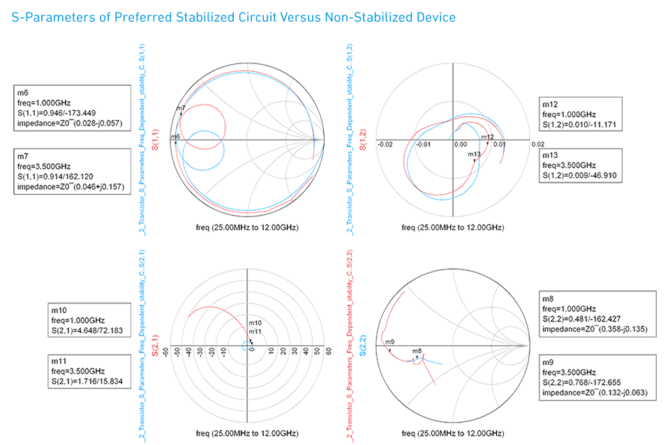 Figure 16.
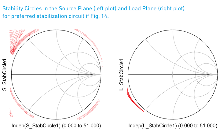 Figure 17.
Key results
So, what are the key findings? As shown in the below data, stability and gain are optimized when using frequency-dependent stability.
- No stabilization – 18.373 dB maximum available gain at 3.5 GHz – Figures 2 and 3 - Unconditionally stable above 1.85 GHz - Conditionally stable below 1.85 GHz
- Resistive stability applied – 12.334 dB maximum available gain is at 3.5 GHz – Figures 6 and 7 - Unconditionally stable over entire 0.025 to 12 GHz frequency range - 6 dB maximum available gain degradation
- BEST RESULT – Frequency-dependent stability applied – Figures 14 and 15 - 17.0 dB maximum available gain at 3.5 GHz - Unconditionally stable over entire 0.025 to 12 GHz frequency range - Increase in maximum available gain of 4.7 dB above resistive stability @ 3.5 GHz
Summary
Modeling helps address common design problems such as stability prior to testing your application on the bench. By accurately modeling and implementing stability techniques, we can match and tune for optimal S-parameter performance while maintaining unconditional stability.
As a final note, the stabilization networks explored here used ideal lumped elements. In an actual microwave design, you will need to include microstrip interconnects and accurate parasitic models for all RLC components, whether you are doing a MMIC design or a board-based hybrid design with lumped elements.
Modelithics Qorvo GaN Library
Learn more about our nonlinear models for packaged and die Qorvo GaN transistors:
- https://www.qorvo.com/design-hub/design-tools/modelithics-qorvo-gan-library
- https://www.modelithics.com/mvp/qorvo
For those with access to the Modelithics Qorvo GaN Library, you can also email info@modelithics.com to request an example ADS workspace and/or NI AWR project related to this blog.
References
- Guillermo Gonzales, Microwave Transistor Amplifiers: Analysis and Design, Second Edition, Prentice-Hall, 1997.
- M. L. Edwards and J. H. Sinsky, "A new criterion for linear 2-port stability using geometrically derived parameters," IEEE Transactions on Microwave Theory and Techniques, Vol. 40, No. 12, pp. 2303-2311, Dec. 1992.
- A. Suarez and R. Quere, Stability Analysis of Nonlinear Microwave Circuits, Artech House, Norwood, MA, 2003.
Have another topic that you would like Qorvo experts to cover? Email your suggestions to the Qorvo Blog team and it could be featured in an upcoming post. Please include your contact information in the body of the email.
