Model-Based GaN PA Design Basics: The What and Why of Intrinsic I-V Waveforms
October 2, 2018
This is the third blog in an ongoing series looking at the importance of GaN HEMT nonlinear models for rapid power amplifier (PA) design success.
In simple linear RF/microwave amplifier design, you can use single-bias S-parameter data to design matching networks that, for example, maximize the gain at a narrow frequency band or achieve a flat gain over a bandwidth.
For gallium nitride (GaN) PAs, designers need to account for nonlinear operation, including what happens with RF current-voltage (I‑V) waveforms. One way to optimize a design for nonlinear behavior is by simulating the intrinsic I-V waveforms. This blog covers:
- What we mean by I-V waveforms
- PA classes of operation
- Intrinsic versus extrinsic I‑V waveforms
- The “waveform engineering” approach to PA design
Catch up on the other blogs in this series:
I-V curves vs. I-V waveforms: What’s the difference?
In a typical GaN HEMT amplifier application, the source is grounded and the RF input signal is applied across the gate-to-source terminals. The drain is connected to the load, and the load impedance determines the load-line trajectory that is traversed as the RF-AC input signal swings back and forth between minimum and maximum peak values.
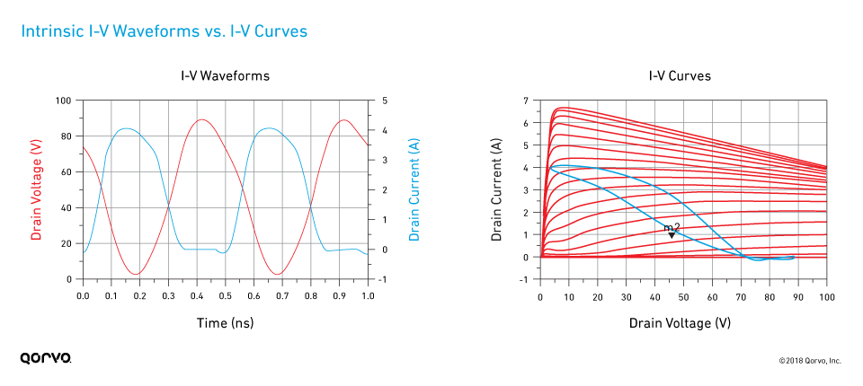
We covered the basics of I‑V curves and load lines in our previous blog in this series, but another way to analyze the nonlinear behavior of a device is by looking at the device’s I-V waveforms — that is, by looking at the current and voltage graphs plotted over time, as shown in the figure below for a 2 GHz input RF signal.
I‑V waveforms and I‑V curves show different information. To illustrate this, we generated the example below using Keysight ADS and the Modelithics Qorvo GaN Library model for the QPD0060, a 90 W, 48 V Qorvo GaN transistor. (We assume sinusoidal signals for our purposes here.)
- The left plot shows the I‑V current and voltage waveforms vs. time for a Class AB bias of Vds = 48 V and Vgs = ‑2.5 V (corresponding to marker m2 in the below right plot).
- The right plot shows the I‑V curves (Ids vs. Vds parameterized on Vgs) in red for Vgs swept from ‑4.5 V to 0 V. The blue curve on the right is called the dynamic load-line and represents the trajectory of the dynamic current-voltage condition at the drain-side current generator as the signal completes a full sine-wave cycle.
I-V waveforms and PA classes of operation
In PA design, “class” is a term used to describe the design approach for the amplifier. This mainly consists of the bias condition and operating mode of the transistor as the output signal is driven to its intended power level.
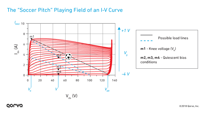
Three of the most basic classes are Class A, Class AB and Class B. As shown in the following figure, these modes correspond to biasing the transistor at the quiescent voltage-current points indicated by markers m2, m3 and m4 for PA classes A, AB and B, respectively.
You can also consider these classes of treatment from an I-V waveform perspective. The following figure shows the results of an intrinsic I-V waveform simulation for Class A, AB, B and C at a 2 GHz fundamental frequency. These simulations were performed using Keysight ADS and the Modelithics Qorvo GaN Library model for QPD0060.
Design Tip: See the end of this blog post for the ADS schematic setup used for the following waveforms.
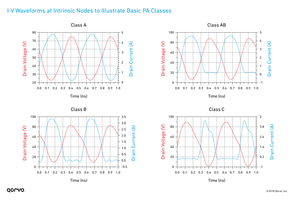
Let’s examine the expectations and nuances of these intrinsic I‑V waveforms:
- Class A: We’d expect that the current and voltage will both essentially be sinusoidal waveforms for signal levels up to the point where either the current or voltage waveform (or both) experiences clipping at the edges of the I‑V “soccer field” limits. This is consistent with the waveform shown in the figure above, and both current and voltage shapes are sinusoidal in shape. Since the current is conducting (nonzero) during the full 360‑degree period of the sine wave cycle, Class A is sometimes referred to as having a “conduction angle” of 360 degrees.
- Class B: For nonclipped signals, we’d expect there to be a full sine wave for the voltage waveform and a half-rectified sine wave for the current waveform. Since we are biased right at the pinchoff voltage for Class B, we expect the current to be nonzero, or conducting, for exactly half of the period of the sine wave; as a result, the conduction angle for Class B is 180 degrees. In the above figure, we can see the current is a half-sinusoid that clips at 0 A during half the cycle. Some nonsinusoidal distortion can be seen in the voltage waveform.
- Class AB: The bias is set to just above pinchoff, so the current is conducting for a little over one-half of the sine-wave cycle of the voltage. For Class AB, the conduction angle is between 180 and 360 degrees. The simulated Class AB waveform shows a sinusoidal voltage and half-sinusoidal current with minimal distortion. The current is seen to conduct for more than half of the cycle.
- Class C: The bias is set to be less than pinchoff, so the current is conducting for less than half of the sine-wave cycle of the voltage. For Class C, the conduction angle is less than 180 degrees. This class is often used in the peaking side device of a Doherty amplifier. In the simulated waveform, the current clearly is conducting for less than half of a sine-wave cycle and the voltage is also distorted and starting to clip on the low-voltage part of the swing.
Two other classes of PA operation are Class F and Class J, which are for more advanced modes of operation that focus on higher efficiency as a primary goal:
- Class F: The voltage is actually squared by reflecting the third harmonic at an appropriate phase and amplitude such that the current/voltage overlap is further minimized. The device is biased at the Class B bias point and harmonic tuning is employed in the matching network. When accomplished correctly, this can produce a PA design with significantly enhanced power-added efficiency (PAE).
- Class J: Class J represents a range of
operating modes that are realized by using a fundamental load with a
significant reactive component, and reactive harmonic terminations that can
be realized with device output capacitance. The device is biased at a
Class B or AB bias point. When accomplished correctly, this can
produce a PA design with significantly enhanced PAE over a reasonable
bandwidth.
The “gotchas” of intrinsic vs. extrinsic ports
The previous figure showed the waveforms for ideal PA classes. But there’s a catch: It makes a difference where you effectively simulate the I‑V waveforms — at the intrinsic or extrinsic port.
It matters because of the device’s parasitics, which could include pad capacitances, bond wires, package parasitics and other factors that impact the performance and design of the device.
The next figure and table illustrate the difference between intrinsic and extrinsic gate, drain and source ports.

| Intrinsic Ports: | Extrinsic Ports: |
|---|---|
|
Establishes the expected waveform behavior for a given set of bias, matching and RF power level conditions. |
Establishes the expected waveform behavior for a given set of bias, matching and RF power level conditions. |
|
Any parasitic parts of the device model (e.g., layout and packaging effects) are considered as part of the external network. |
The parasitic parts of the device model are included in the simulation. |
|
Represents a close approximation to how the RF signal voltages and currents behave. |
Results in distorted waveforms compared to expected behavior for various PA classes. |
|
Are constrained by the limits of I‑V curves. |
Simulated dynamic load-line behavior will not remain constrained to the limits of I‑V curves (see the next figure below). |
|
When done properly, this will result in expected, nearly idealized behavior for basic and advanced PA class waveforms. |
Extrinsic waveforms readily extend into the “out of bounds” regions of our I‑V “soccer field.” |
|
Can use intrinsic waveforms to optimize PA performance as part of a “waveform engineering” design approach (discussed later in this blog). |
Difficult to use extrinsic waveforms for waveform engineering. |
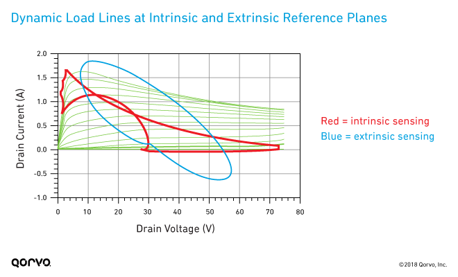
To further illustrate the differences between intrinsic and extrinsic ports, the following image depicts an example dynamic load-line plot for a smaller device “die” format from a simulated GaN HEMT model and shows the trajectory of the intrinsic (in red) and extrinsic (in blue) RF I-V waveforms as the input signal swings through an entire cycle. Note how the extrinsic cycle extends beyond the I‑V curve limits and the current swings negative due to extrinsic parasitic effects.
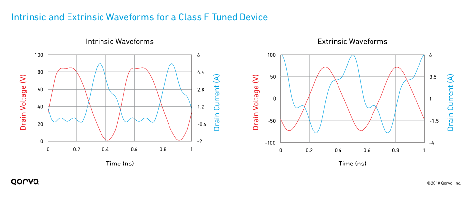
The next figure highlights the difference between intrinsic and extrinsic I‑V waveforms using an example Class F amplifier design:
- For this example, I used NI AWR Design Environment and the same QPD0060 GaN device model used in the previous examples of PA classes.
- I then tuned the third-harmonic load condition to “square” the intrinsic voltage waveform, producing the Class F–shaped waveforms shown.
- From an I-V waveform perspective, this example shows that the intrinsic waveforms follow the expected trends for sinusoidal input signals for a properly biased and matched PA — but the extrinsic waveforms do not.
- The below right plot clearly shows that the extrinsic waveforms are distorted by the parasitic capacitance and inductance of the packaged device.
Design Tip: See the end of this blog post for the NI AWR schematic setup used for the following waveforms.
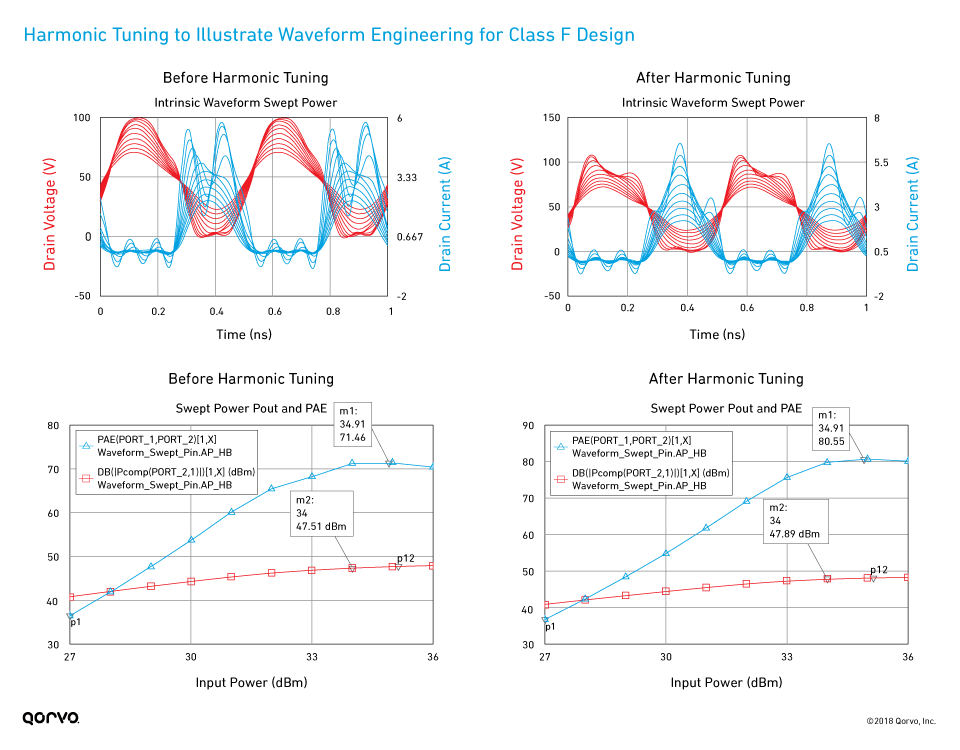
Fine-tuning a Class F PA design example with “waveform engineering”
But what if your intrinsic waveforms don’t reflect the desired I‑V waveforms for your operating class? Harmonic tuning may be the answer.
All of the Modelithics Qorvo GaN Library models allow the circuit designer to monitor the intrinsic voltage and current waveforms while tuning or optimizing the load matching circuit until the desired waveform shaping is achieved. This is sometimes called the “waveform engineering” approach to PA design.
To demonstrate this concept of waveform engineering, the next figure shows power sweep results for the intrinsic I‑V waveforms both before and after harmonic tuning. Compared to the initial Class F waveform plots shown in the previous section, I tuned the fundamental load impedance to optimize efficiency to a value of 71.5%. When comparing the bottom two plots, note the following:
- We see nine points of improved efficiency to 80.5% after also tuning the third harmonic and “squaring the voltage.”
- The efficiency improvement was done at no change to the achieved power level of 34.9 dBm.
Design Tip: See the end of this blog post for the NI AWR schematic setup used for the following waveforms.
The takeaway: Simulate at intrinsic nodes to maximize your GaN PA design
In summary, extrinsic waveforms aren’t useful for design because they aren’t constrained by the limits of the I‑V curves — and it is precisely these current/voltage constraints that determine the power capability of a device at a given set of bias/current/matching conditions.
It’s better to simulate I‑V waveforms for your design at the intrinsic ports. Simulating the intrinsic I‑V waveforms is key to:
- Optimizing matching networks
- Compensating for distortions caused by device parasitics
- Achieving optimal power and efficiency
- Attaining first-pass design success
You can then use waveform engineering to further fine-tune the design and
performance of your device for your specific application.
Featured Article: Waveform
Engineering
Read this article describing a PA design flow using the Qorvo T2G6000528 GaN HEMT, NI AWR and the
Modelithics Qorvo GaN Library:
- Designing a Broadband, Highly Efficient, GaN RF Power Amplifier (Microwave Journal)
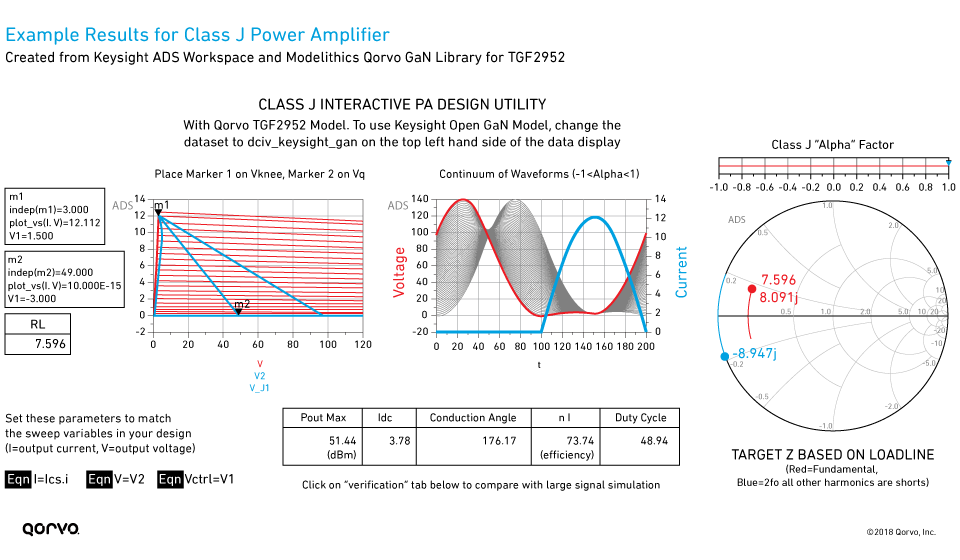
Go in depth: Tutorial video and downloadable workspace for Class J PA design
Models, such as those in the Modelithics Qorvo GaN Library, that include access to the intrinsic voltage-current ports are required to enable designers to optimize the I-V waveforms for high-efficiency classes, such as Class F and other advanced PA operating modes (including Class E, Class J and inverse Class F) that designers are utilizing to meet the complex linearity and efficiency specifications of today’s challenging designs.
You can see a nice example that illustrates the use of intrinsic waveforms for a Class J amplifier design in a YouTube how-to video developed by Matt Ozalas of Keysight. The tutorial also includes an interactive Keysight ADS workspace you can download. The following figure is a screenshot of results from Matt’s Class J example using a Modelithics model for the Qorvo TGF2952 GaN transistor.
In the next part of this series, we’ll discuss how you can use
models to simulate S-parameters and explore resistive stabilization that is
often required for successful RF PA design.
Modelithics Qorvo GaN Library
Learn more about our nonlinear models for packaged and die Qorvo GaN transistors.
For those with access, you can also email info@modelithics.com to request an example ADS workspace and/or NI AWR project related to this blog post.
Schematic Setups
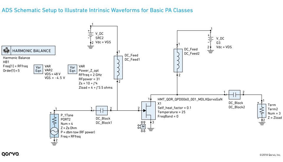
I‑V Waveforms for Basic PA Classes A, B, AB and C: The following figure shows the schematic setup used to simulate the four basic PA class I‑V waveforms, with conditions set for the Class C case. These simulations were performed using Keysight ADS and the Modelithics Qorvo GaN Library model for QPD0060.
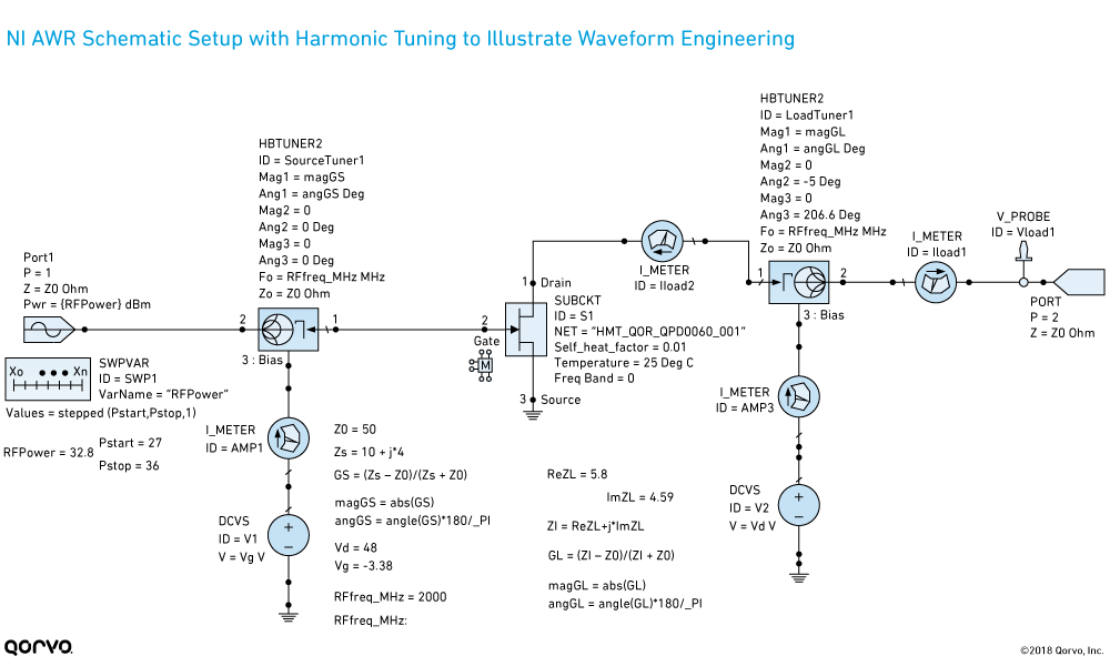
Harmonic Tuning to Illustrate Waveform Engineering for Class F Design: The following figure shows the schematic setup used to simulate intrinsic and extrinsic waveforms as well as power and efficiency under swept input power at a 2 GHz fundamental frequency. These simulations were performed using NI AWR and the Modelithics Qorvo GaN Library model for QPD0060.
Have another topic that you would like Qorvo experts to cover? Email your suggestions to the Qorvo Blog team and it could be featured in an upcoming post. Please include your contact information in the body of the email.