Model-Based GaN PA Design Basics: What’s in an I-V Curve?
May 31, 2018
This is the second blog in a series explaining various aspects of model-based power amplifier (PA) design. Part 1 covered the basic concepts of a nonlinear GaN model.
As a relatively newer technology, gallium nitride (GaN) requires some different techniques and thinking than other semiconductor technologies.
For those new to GaN PA design, an understanding of I-V
curves (also known as current-voltage
characteristic curves) is a good place to start. This blog examines the
importance of I-V curves and how their representation within a nonlinear GaN
model, like those in the Modelithics
Qorvo GaN Library, can help make your design process more accurate and
efficient.
GaN: The Basics
Brush up on your knowledge of GaN.
What’s the pitch?
You can think of I-V curves a little like a soccer field — sometimes called a "pitch" — where the limits dictate the boundaries for the microwave signal, as shown in the figure below. In simple terms, once you hit the boundary, you get signal clipping, which causes compression and nonlinear distortion. The boundaries are set by the following:
- The knee voltage and maximum current (Imax), indicated by the corner marker m1 in the figure
- The zero-current line corresponding to the gate-to-source pinchoff voltage (Vpo)
- The breakdown voltage (VBR) indicated by the curling up of the current line on the right
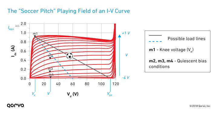
Knee voltage, bias conditions and gain
The figure also shows the following:
- Marker m1 indicates the knee voltage (Vk).
- Markers m2, m3 and m4 indicate nominal quiescent bias conditions representing Class A, AB and B conventional PA operating classes or modes, respectively. To be sure, there are other modes — for example, Class C bias corresponds to a gate voltage more negative than the pinchoff voltage and consequently has RF current flowing for less than half a cycle of the input gate voltage waveform.
Remember: For GaN devices, the pinchoff voltage is always a negative voltage. Learn more >
The various curves represent different values of the gate to source voltage, from pinchoff (in this case, about ‑4 V) to slightly positive values (Vgs = 1 V). For this device, note that the absolute maximum current allowed (Imax) is about 900 mA, and the breakdown voltage (VBR) is around 118 V.
The spacing of the I-V curves for different values of Vgs is
related to what is called the transconductance
(gm ≈ ΔIds/ΔVgs), which in turn is related to
the gain. (In this figure, the Vgs step voltage is 0.2 V.)
Notice that in the vicinity of m4 (Class B bias), the curves
are more closely spaced compared to m3 (Class AB). This
is one reason Class AB, which has similar efficiency advantages as
Class B, is often preferred due to higher gain.
Glossary of Notations
Ids: drain-to-source current
IdsQ: drain-to-source quiescent current
Imax: maximum current
VBR: breakdown voltage
Vd: drain voltage
Vds: drain-to-source voltage
VdsQ: drain-to-source quiescent voltage
Vg: gate voltage
Vgs: gate-to-source voltage
VgsQ: gate-to-source quiescent voltage
Vk: knee voltage. The place in the I-V curve where the voltage goes up.
Vpo: pinchoff voltage. The specific point when the device is off at a particular voltage. For GaN, pinchoff is a negative voltage.
How much RF power can I get?
The figure above also shows a dashed blue line and a solid dark gray line to indicate possible load-lines along which an AC signal would swing back and forth. In an ideal sense, the dark gray line allows for maximum use of the I-V “playing field” and would allow a signal to make use of the maximum current and maximum voltage swing.
In this example, the quiescent bias voltage might in principal be set to 61 V. However, for reliability and design margin reasons, I’d recommend a lower nominal bias voltage (always less than half the breakdown voltage) and different optimal load-line (here we chose 28 V, marked m2, m3 and m4 in the figure above). A simple rough estimation of the power potential of the device (for Class A and B) can be provided as 0.25*(VdsQ-Vk)*Imax. For the device shown here, this comes out to be about 5 W.
For a given process, the breakdown voltage tends to be constant, so you can obtain more power by increasing the gate width. This leads to a common metric for power capability called power density, which for GaN is on the order of 5-10 watts per mm (W/mm) of gate width, compared to 0.5 to 1 W/mm for GaAs transistors.
In simple terms, to maximize current/voltage peaks before clipping and
thereby optimize power output, the load resistance would be the reciprocal
of the load-line slope (neglecting device and package reactive parasitic
effects). This optimal power load invariably is different than that needed to
maximize the gain of the device derived from linear circuit theory.
GaN’s ability to expand the I-V “playing field”
Coming back to our simple estimation of power capability, 0.25*(VdsQ-Vk)*Imax, you see we can get more power by using the following:
- Devices with higher Imax
- Devices that can operate at higher quiescent voltages
- Devices that can do both (higher Imax or VdsQ)
Commercial GaN processes have breakdown voltages between 100 V and
200 V, an order of magnitude higher than GaAs breakdown voltages and
also over twice that of typical LDMOS processes. GaN effectively expands the
boundaries of the I-V playing field mentioned earlier, and this expansion of
the I-V curves is what makes the technology so exciting for high-power PA
design.
Are there any traps we should worry about?
Trapping is an electrical phenomenon that affects both GaAs and GaN HEMT device operation. It occurs in the epitaxy layers of the device, where electrons that could be available to enhance current flow in the HEMT channel become essentially “trapped” in defect states occurring at the surface or within the GaAs or GaN lattice. This trapping is voltage dependent and degrades the device’s operation over time, affecting parameters such as the knee voltage.
One of the well-known consequences of trapping in GaN is called
knee walkout, which moves the I-V curve knee voltage toward
the right, as shown in the following figure.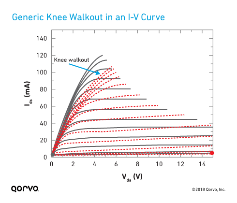
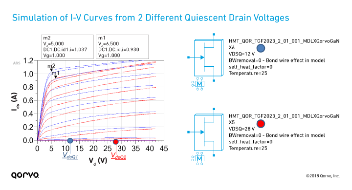
The good news is that nonlinear GaN models can help predict this trapping behavior. The figure below shows the I-V curves for one of the Qorvo die models, as captured in the Modelithics Qorvo GaN Model. It shows the simulation of two different quiescent drain voltages (12 V and 28 V, marked VdsQ1 and VdsQ2 below) under short pulse conditions (e.g., 0.5 µs pulse width at a duty cycle of 0.05%).
Note how both the knee voltage and Imax are affected by this trap-related knee walkout effect. With the self_heat_factor input set to zero, this model data recreates very well the I-V curves that were measured under short pulse conditions from 12 V and 28 V quiescent drain voltage (with VgsQ set to pinchoff).
As we know from the above discussion, both parameters in turn affect the maximum power potential of the device — so the model’s ability to track I-V changes with operating voltage can be quite important depending on the application.
Nonlinear models can speed up the design process
It’s important to understand the impact and nuances of I-V curves and, in turn, their fundamental limitations and impact on PA design. If you are new to this field, hopefully this blog has helped you appreciate that there really is a lot of useful information in an I-V curve!
Choosing load conditions that maximize large-signal power capability is quite different from linear conjugate match thinking — and using nonlinear GaN models during the design process can help you to get the design right the first time. Rather than primarily worrying about matching to the output impedance of the transistor, we need to think in terms of how to maximize the current and voltage swing across the I-V “playing field,” which is governed by the boundaries of the I-V curves from the knee voltage and maximum current down along a chosen load-line to the pinchoff region.
Download our brochure or visit our Modelithics Qorvo GaN Library page in the Qorvo Design Hub to learn more about our nonlinear models for Qorvo GaN transistors. You can request free access at https://www.modelithics.com/requests/qorvogan.
Note: The first and last example images in
this blog are recreated based on images output from the Modelithics Qorvo
GaN Library.
Have another topic that you would like Qorvo experts to cover? Email your suggestions to the Qorvo Blog team and it could be featured in an upcoming post. Please include your contact information in the body of the email.