Revolutionizing Radar Design with Electronically Reconfigurable GaN
Power Amplifiers
June 14, 2021
This post first appeared in Microwave Product Digest.
This article demonstrates for the first time a robust commercially available high power amplifier based on multi-band transmitter design using a patented reconfigurable PA technique demonstrated by Charles Campbell [2,3,4]. The reconfigurable PA has single-input and single-output reconfigurable matching networks depending on control bit settings for each band of interest. Each bit setting configures all matching networks for band specific optimum performance, enabling the PA to deliver the best system level performance possible in a compact package. This results in an overall reduction in size and weight. This new reconfigurable PA design approach overcomes multiple shortcomings of traditional multi-band transmit front-end designs. The most obvious benefit is the elimination of a band select switch at the PA output. This reduces the output loss by 0.8-1.0 dB, giving it a clear advantage over traditional design approaches. If designed with optimum load impedances and smart switch placement, the reconfigurable PA can closely approximate the performance levels achieved by independently tuned band specific amplifiers.

Modern radar systems are being configured as multi-band radars that can use multiple frequency bands in various environment and target conditions to interpret complex scenes. These systems provide an unprecedented level of performance and capability to detect and track hostile targets. For example, Dual Band Radar (DBR) is the first radar system in the U.S. Navy fleet capable of simultaneously operating over two frequency bands (S/X-bands), coordinated by a single resource manager [1]. S-band signals are resistant to severe weather and atmospheric attenuation. On the other hand, X-band frequencies are often used for highly resolved target imaging. Most current power amplifiers (PAs) are not suitable for multi-band radar systems because the desired frequency bands are far apart, and individual PAs are optimized at each target frequency band. There have been several approaches to implement broadband or multi-band characteristics by switching between individual PA MMICs. These approaches use either wideband non-uniform distributed PA (NDPA) covering both bands or dual passband power amplifier designs.
The benefits of a reconfigurable PA are more evident when compared to a wideband amplifier. In wideband amplifier design, load impedance is typically designed to be below optimum load target to achieve high output network bandwidth. Wideband amplifiers have reduced output power and power added efficiency (PAE). Therefore, the ability to synthesize optimum load impedances is key to reconfigurable PA design. The consequence of this is the ability to increase amplifier field-effect transmitter (FET) periphery, maximizing output power within thermal limits. These design principles have been implemented in Qorvo's novel product, QPA0007. The QPA0007 is a 30 Watt S/X-band reconfigurable power amplifier using Qorvo's 150 nm gate length GaN HEMT process technology (QGaN15). Summary of reconfigurable amplifier comparison against wideband and traditional multi-band approach is shown in Figure 1.
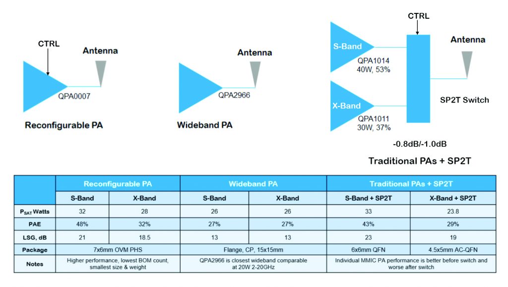
Figure 1: Multi-band power amplifier front-end comparison
Process and Package Technology
Qorvo's QGaN15 process technology is ideal for X-band higher power PA designs. It offers fast transistors with high gate to drain breakdown for high power applications. QGaN15 comes with multiple process options for different circuit applications. In the case of QPA0007, a proprietary process technique was implemented to improve device and circuit performance. The use of a top metal layer enables the use of narrower output matching traces, reducing the physical area significantly while maintaining metal current density design rules. The output network loss is not very sensitive to the metal thickness. At X-band, the use of passivation reduces circuit performance but enables the use of cost-effective packaging. A secondary benefit of using a passivation layer over the die is that it helps with both FET and passive network modelling accuracy compared to just using an overmolded package without passivation. Higher circuit performance could be achieved by eliminating the need for passivation by using a more expensive air cavity package.
The QPA0007 uses cost efficient overmolded 7mm x 6mm Plated Heat Spreader (PHS) package technology. PHS package is very flexible to design with and offers designers a good thermal path under the die for medium output power devices. Wide input and output connections and generous pad spacings enable high yield PCB attachment. On the evaluation board (EVB), the control pins as well as gate pins can be connected either from the top or bottom sides. Robust drain connections need to be connected from both sides. The QPA0007 package pinout and footprint as well as evaluation board are illustrated in Figure 2.
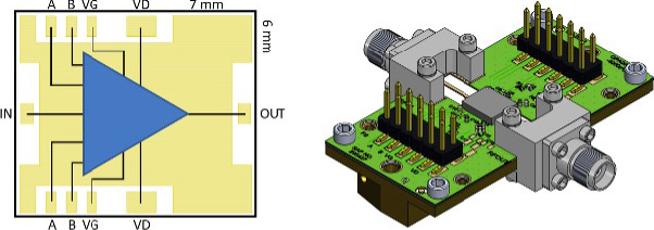
Figure 2: QPA0007 PHS package and evaluation board
Circuit Design
Fundamentally, the QPA0007 is a two stage reactively matched power amplifier. The band switching is implemented with switchable capacitors and inductors controlled by on-chip level shifters adjusting the switch FET bias levels. Each network is designed to maintain an optimum load for both bands independently. This requires small tradeoffs compared to band specific designs. The output network loss is one of the critical design parameters and is impacted by switch losses. Fortunately, these switch losses are minor compared to having a separate band select switch at the PA output. The number of tuning switches is minimized, not only from the overall loss perspective but also from the complexity and size perspective. Generally, to achieve low switch loss, switch periphery tends to get large and therefore has high off capacitance. Off capacitance plays an important role in the effectiveness of a switching element. This limits the usability of switchable shunt capacitors in the output network. Typically, tuning inductance is much larger at S-band than at X-band. In the signal path, it is not worth using series switches to tune series inductance due to extra switch loss, but rather make small compromises in achieving close to optimum load target.
The design environment is different for the interstage matching network compared to output network. The interstage matching network is bandwidth and space constrained rather than loss constrained. Therefore, smaller switches can be used in multiple places to achieve optimum load target.
When comparing output and interstage networks, the input network has the most flexibility due to relaxed loss requirement and having space for more switches and control signals. Both input and interstage networks play a role in amplifier stability performance. Additional loss is added to guarantee stability over wide operating conditions, especially at extremely cold conditions. Tuning capacitors and FET terminals have been designed to withstand high voltage standing wave ratio (VSWR) load conditions at maximum input drive to avoid breakdown.
Finally, the overall design challenge is to limit S-band small signal gain while not destroying X-band gain. S-band performance is helped by lower frequency FET performance, but limited by the difficulty of extending low-end bandwidth without sacrificing X-band performance. This is a real challenge even with switchable tuning elements.
Performance
The QPA0007 is tuned to cover S-band 3.1-3.5 GHz and X-band 9-11 GHz. Two band switching signals are complementary 0 V and -10 V for S-band and -10 V and 0 V for X-band. The control signals draw or sink 5 mA depending on band selection.
QPA0007 quiescent bias is 700 mA from 26V. Since the input power drives up drain current, output power and PAE are highly independent of quiescent bias current. Therefore, quiescent bias current can be set based on other performance parameters like small signal gain and switching times.
All the reported measurement results were obtained from the production EVB calibrated to QPA0007 input and output pins. Measured small signal gain is 27 dB for S-band and 23 dB for X-band at 25°C. This difference in small signal gain reflects the change in FET performance across the frequency band. Input return loss is above 20 dB for S-band and 10 dB for X-band. Measured S-parameters are shown in Figure 3.
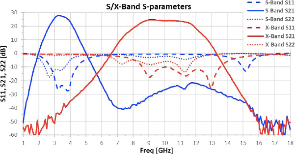
Figure 3: QPA0007 S/X-Band S-parameters
At S-band, the QPA0007 delivers 45 dBm of output power with 48% PAE. Large signal gain at optimum operating point is 21 dB and draws 2.6 A. At X-band, output power is 44.5 dBm and PAE 32%. Large signal gain is 18.5 dB drawing 3.6 A. These results have been measured with 100 µs/1 ms drain pulse. S/X-band large signal performance plots are shown in Figure 4
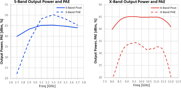
Figure 4: S/X-Band output power and PAE
Harmonics have been measured into 50 ohm load. S-band 2nd harmonic is below -25 dBc and 3rd harmonic -25 dBc. X-band 2nd and 3rd harmonics are -35 dBc and -55 dBc, respectively.
The QPA0007 has been tested for both small signal and driven stability to VSWR 10:1 loads at -40°C. Device robustness has been tested with extreme input drive to VSWR 3:1 loads at 85°C without any performance degradations.
Switching times can be categorized in two groups: RF signal turn on without band switching and band switching with simultaneous RF turn on. In real applications, band switching with simultaneous RF turn on might not be required, but this illustrates the capability of the device. Switching time within band is less than 100 ns. Band switching with simultaneous RF turn on is below 1 µs. RF turn off is practically instantaneous in both use scenarios.
Power dissipation at S-band is 40 W and X-band is 70 W during 100 µs pulse width and 1 ms pulse period. Pulsing can be done either by using drain pulse or RF pulse. This type of pulsing characteristic keeps the device junction temperature below long-term reliability limit at 85°C base plate temperature. Comprehensive thermal analysis has been done to validate thermal conclusions based on measured data. The QPA0007 is fully production qualified with MSL 3 and HBM 250V rating. Measured EVB results are summarized in Table 1.
| S-Band | X-Band | |
| Frequency | 3.1 - 3.5 GHz | 9 - 11 GHz |
| Output power | 45 dBm (32W) | 44.5 dBm (28W) |
| PAE | 47% | 32% |
| Small signal gain | 27 dB | 23 dB |
| Large signal gain | 20.5 dB | 18.5 dB |
| Input return loss | 20 dB | 10 dB |
| Output return loss | 9 dB | 5 dB |
| Bias | 0.7A @ 26V | 0.7A @ 26V |
Summary
The reconfigurable multi-band power amplifier approach demonstrated in this paper has clear advantages over traditional band switching power amplifier front-ends. Qorvo's QPA0007, based on this patented technology, is first in the industry to demonstrate improved output power and efficiency performance at both S/X-bands using the same device. In addition, the QPA0007 offers customers a competitive form factor in a cost-effective high-volume package.
Acknowledgments
The authors would like to thank Terry Hon, Paul Prudhomme, Gregory Clark, Sujo Vegus, Gary Petree and Reilly Martinez for their individual contributions and excellent support.
References:
[1] https://www.raytheon.com/capabilities/products/dbr
[2] Campbell, C. F., et al. “Electronically reconfigurable matching network.” U.S. Patent 10,164,587, issued December 25, 2018.
[3] Campbell, C. F., Kobayashi, K. W. and Lee, C. “A Reconfigurable S/X-Band 25W GaN Power Amplifier MMIC”, 2019 GOMAC-Tech.
[4] http://imapsne.org/virtualCDs/2019/2019%20Presentations/C/C2.pdf
Have another topic that you would like Qorvo experts to cover? Email your suggestions to the Qorvo Blog team and it could be featured in an upcoming post. Please include your contact information in the body of the email.