Advanced Packaging: Qorvo's Centers of Excellence
Qorvo runs centers of excellence that design, manufacture, assemble and package our products. These facilities provide the quality, confidence and speed that our customers count on around the world.
Trusted by NASA and accredited by the U.S. defense industry, Qorvo provides a technology portfolio that is unmatched in the industry. We pioneered and perfected many of today's leading processes with GaN, GaAs and other materials that enable the highest-performing, smallest and most cost-effective RF modules on the market. Our innovation and expertise also speed prototyping, reducing our customers’ time to market.
Featured below is information about three of our manufacturing facilities in the U.S. and China, and their expertise. Additional manufacturing locations include Hillsboro, Oregon; Apopka, Florida; Greensboro, North Carolina; San Jose, Costa Rica; and Nuremberg, Germany.
U.S.-Based Center for Defense and Communications
Qorvo's defense and network communications customers receive comprehensive manufacturing services from our Advanced Microwave Module Assembly facility, also known as "AMMA."
AMMA provides a "one-stop shop" for Qorvo's design, manufacturing, assembly and packaging. Located just north of Dallas, Texas, this world-class facility provides advanced, integrated assembly and packaging of RF components within communications, radar and electronic warfare (EW) applications.
In fact, Qorvo designs and fabricates custom products for strategic customers. Our strong applications teams design future new products and solutions that address our customers' toughest challenges.
Complementing our processing and sourcing expertise are the industry's best and most cost-effective assembly and packaging technologies. With the addition of die-attach equipment, we fabricate, test, package and ship die-level devices to customers from one secure location.
To meet customer needs, we offer a wide variety of high-reliability RF packaging options including ceramic, our in-house plastic epoxy packaging, military-grade and high-grade custom metal packaging, and more.
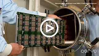 Qorvo Advanced Microwave Module Assembly (AMMA)
Facility. Watch the Video
Qorvo Advanced Microwave Module Assembly (AMMA)
Facility. Watch the Video
Capabilities
Secure Facility
Fabricate circuits, package die, and test components in one convenient location for shorter lead times and greater savings. Site accredited as a Category 1A Trusted Source by U.S. Dept of Defense.
Single- and Multi-Chip Assembly
Integrate single or multiple die using industry-standard or custom packages.
Experience and Innovation
Ensure your program success through Qorvo's expert teams and state-of-the-art facilities.
Cost-Effective Manufacturing
In 2015, Qorvo scaled our gallium nitride on silicon carbide (GaN-on-SiC) process to produce MMICs on 6-inch wafers. Transitioning from 4-inch to 6-inch wafers serves to nearly double GaN-on-SiC
manufacturing capacity — accelerating the affordable manufacture of RF devices.
Die-on-Tab (DoT)
Simplify assembly, increase yields and mitigate thermal considerations through virtually void-free vacuum reflow die attach. The DoT process attaches die-level devices to thermal spreaders for easier handling.
All devices are 100% in-factory X-ray inspected.
Bottom line, Qorvo's packaging expertise expands our portfolio of integrated solutions, providing convenience and lowering overall system costs.
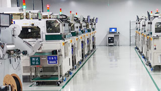
Asia-Based Packaging for High-Volume Customers

In China, Qorvo runs two centers of excellence in Beijing and Dezhou. These facilities provide high-volume manufacturing, assembly, packaging, and thorough qualification and reliability testing.
Serving a large, global customer base, our Beijing and Dezhou facilities excel in high-volume production. With its state-of-the-art equipment and automated manufacturing processes, Qorvo has developed capabilities to assemble and test packages such as such as low-pin count QFN, TSSOP and other common ones.
With the increased complexity and miniaturization of RF devices, Qorvo focuses on multi-chip module (MCM) packaging, which helps customers reduce board space by up to 50 percent. Our MCM packaging enables up to 30 percent cost savings versus traditional SOT115J packaging. MCM packaging features temperature-sensing pins, which ensure proper assembly and provide optimal thermal management for mobile devices.
Capabilities
- Beijing: 18,350 square meters of space used for production since 2001
- Dezhou: 22,475 square meters of space used for production since 2015
- Microshield™ installed; qualification and initial production release in progress
- WLCSP probe / DPS qualification (estimated completion in 2016)
- Cu-pillar bump setup in progress, qualification (estimated completion in 2016)
- Proprietary CuFlip™ (copper flip) and WLP (wafer level packaging) technology
Awards and Accreditations